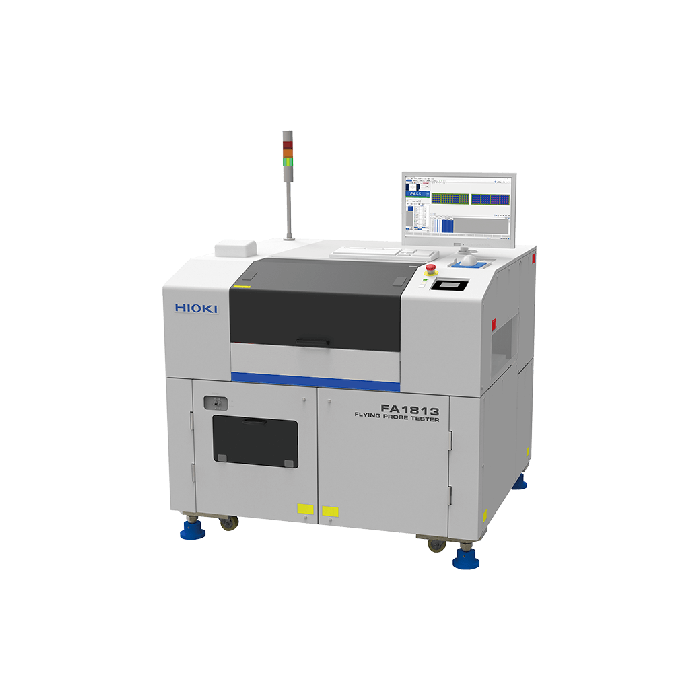
FA1813
FA1813
Hioki
Flying Probe Tester
Flagship model for package board testing
Upper arm board alignment uses a high-resolution camera with twice the pixels as the previous model and a high-magnification lens (with 2× optical zoom) to help achieve accurate probing of the fine-pitch pads found on high-density package boards.
“Probe-down with contact check,” a new function, facilitates optimal probe stroke to minimise impact marks, reducing damage to pads.
Key Features
- Four-terminal measurement of fine-pitch pads
- Reduced impact marking when used with the latest probes
- Defect analysis using Process Analyser
Click below to request a quote for this item. Or for product advice, stock and lead time enquiries call our team on 0330 313 3220.
| Attribute | Value |
|---|---|
| Power Supply | 200 V, 220 V, 230 V, 240 V AC single-phase (specify at time of order), 50/60 Hz, 5 kVA |
| Measurement Speed | Max. 76 points/ s (X-Y movements of 0.15 mm, 4-arm simultaneous probing, when capacitance measurement) |
| Number Of Arms | 4 (2 each, top and bottom) |
| Compatible Probes | 1172 series, 1072 series, 1073 series |
| Number Of Test Steps | Max. 999,999 steps |
| Test Parameters And Measurement Ranges |
Resistance: 40.00 μΩ to 100.0 MΩ Constant DC current continuity measurement: 400.0 m Ω to 1.000 k Ω Constant DC current resistance value measurement: 40.00 μ Ω to 400.0 K Ω Constant DC voltage resistance value measurement: 4.000 Ω to 40.00 M Ω Insulation resistance: 1.000 kΩ to 100.0 GΩ Capacitance: 100.0 fF to 10.00 μF Leak current measurement: 100.0 μA to 10.00 mA High voltage resistance: 1.000 kΩ to 100.0 GΩ Capacitance Insulation resistance: 1.000 kΩ to 10.00 MΩ Open test: 4.000 Ω to 4.000 MΩ Short test: 400.0 mΩ to 40.00 kΩ LSI Connection test: 0.000 V to 12.00 V Measuring resistance: 10.00 Ω to 100.0 k Ω Measuring capacitance (For parts inspection): 10.00 p F to 100.0 μ F Inductance: 1.000 μH to 1.000 mH |
| Judgment Range | -99.9% to +999.9% or absolute value Minimum resolution of XY movement 0.1 μm/pulse Minimum resolution of Z movement 1 μm/pulse |
| Minimum Pad Pitch |
Top surface: 32 um (with CP1075-09) Bottom surface: 44 um (with CP1075-09) |
| Minimum Pad Size |
Top surface: 2 um (with CP1075-09) Bottom surface: 14 um (with CP1075-09) |
| Testable Board Size |
Thickness: 0.5 mm (0.02 in) to 2.5 mm (0.10 in) Outer dimensions: 50 mm (1.97 in) W × 50 mm (1.97 in) D to 400 mm (15.75 in) W × 330 mm (12.99 in) D |
| Maximum Testable Area | 398 mm (15.67 in) W × 304 mm (11.97 in) D |
| Clamp Method | Board 2-side chuck method (with tension function) |
| Attribute | Value |
|---|---|
| Data Sheet | Click here to view |


