Electrostatic Discharge (ESD) Testing for EMC Immunity
Test levels, waveform requirements and in-house lab setup for static discharge compliance
Electrostatic Discharge (ESD) testing verifies that your product can withstand the real-world static events people barely notice. A tiny shock that feels like nothing to a human can cause critical, invisible damage inside electronic components. These failures are often undetectable during assembly, yet they can lead to resets, malfunctions or complete breakdowns once the device is operating inside real-world applications, including critical environments such as medical, defence, aerospace and industrial systems where unexpected failures can’t be tolerated.
This guide will walk through what ESD testing is, how it works, the EN 61000-4-2 test standard and the specific equipment required.
We will also highlight the cost advantages of replacing outsourced test sessions with an in-house ESD testing facility, giving engineering teams the ability to run tests on demand, reduce retest fees and accelerate product development.
What is ESD testing?
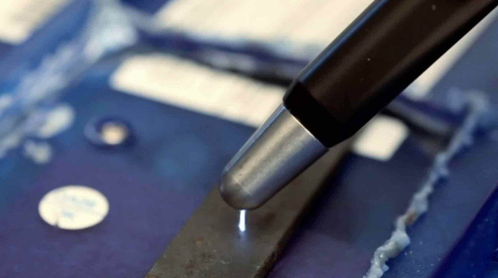
ESD (electrostatic discharge) testing is a method used to determine an electronic device's susceptibility to damage from electrostatic discharge events. It is performed at both the component level, e.g. on integrated circuits and system level to ensure a product can operate reliably without being damaged by ESD strikes that can occur during manufacturing, transportation or normal use. The process uses specialised equipment, such as ESD guns, to simulate various discharge scenarios in accordance with international standards such as EN 61000-4-2.

How does ESD damage components?
- Disruption: Disruption of communication signals critical to device operation
- Heat damage: ESD creates a sudden, high-current spike that produces intense heat. This can melt or vaporise tiny conductive layers inside microchips and transistors
- Electrical breakdown: The high voltage can punch through thin internal structures, like MOSFET gate oxide or transistor junctions
- Physical damage: The discharge can leave visible pits, cracks, or burn marks on silicon and internal conductors
- Latent defects: The component may still work after the event, but hidden damage weakens it, leading to intermittent or future failures that are hard to diagnose
What electronics are commonly affected?
The components most at risk of ESD damage include semiconductors such as transistors and integrated circuits (ICs), thin-film resistors, certain voltage-dependent capacitors and storage devices like hard drives and SSDs. Their small footprint and dense internal structures make them highly susceptible to oxide breakdown, junction damage, open circuits and data corruption during an electrostatic discharge event.
What is ESD?
ESD stands for Electrostatic Discharge, which is the sudden flow of electricity between two objects with different electrical potentials. This is the same "static shock" you feel when touching a doorknob. While it's usually harmless to humans, it can be catastrophic for sensitive electronic components like computer parts. ESD occurs when static charge builds up due to friction, creating a voltage imbalance that discharges when the objects touch.
What is the key purpose of ESD testing, and why is it important?
Once a product enters real-world use, it must withstand routine ESD interactions without performance loss. ESD testing determines how susceptible a device is to electrostatic discharge and verifies that it can continue operating reliably when exposed to sudden, brief electric currents. Any weakness in its immunity levels relative to standards such as EN 61000-4-2 can lead to resets, communication faults, intermittent issues or complete device failure during normal operation.
Key purposes:
- Verify device robustness: ESD testing evaluates how well components, devices, and entire systems can withstand ESD events, such as those that occur from human contact.
- Ensure product reliability and safety: Simulated ESD strikes reveal weaknesses that can lead to both immediate failures and latent ESD effects, hidden damage that may cause intermittent behaviour or premature failure later in the product’s life.
- Test protection systems: It is used to check the effectiveness of ESD protective measures, such as wrist straps and grounding mats, to ensure they are functioning correctly and protecting against static discharge.
- Meet industry standards: Testing helps verify that products meet specific ESD immunity standards, such as EN 61000-4-2 for system-level testing or various standards for device-level tests.
- Identify failure points: By incrementally increasing voltage during a test, it's possible to determine the maximum voltage a component can tolerate before failure occurs, providing valuable design feedback.
What ESD damage really looks like (and why you can’t see it)
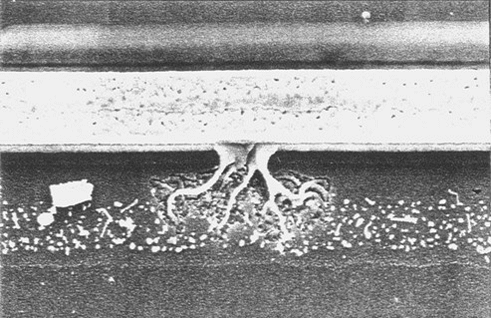
One of the biggest challenges with ESD failure is that the damage is rarely visible to the naked eye. A component may look completely normal externally, even after a severe discharge event. The real damage happens deep inside the device, within semiconductor layers measured in microns.
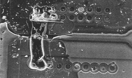
However, when viewed under a microscope, the effects become obvious. ESD can rupture thin oxide layers, melt metal traces, create crater-like blowouts and cause electrothermal migration. These failures range from catastrophic “hard failures” to subtle, latent defects that only reveal themselves later as intermittent resets or unexplained field failures.
The images below illustrate how different types of ESD damage appear under inspection:


Industries where ESD testing is crucial
ESD immunity is essential across sectors that form part of the UK’s Critical National Infrastructure (CNI), including aerospace, defence, medical and automotive systems. These industries rely on proven ESD performance because even a single weak or latent-damaged component can lead to costly, dangerous or mission-critical failures that disrupt essential services and have a major detrimental impact on national security.


Aerospace & Avionics
Aerospace electronics require strong ESD immunity to prevent latent damage that can cause in-flight resets, sensor faults or degraded avionics performance (DO-160G (Section 25)


Military & Defence Electronics
Defence systems need robust ESD protection because hidden damage can cause communication dropouts, targeting errors or unexpected shutdowns
(MIL-STD-461G / CS118)


Medical Devices &
Clinical Electronics
Medical equipment must resist ESD to avoid inaccurate readings and unexpected resets that could compromise patient safety
(EN 60601-1-2)


Automotive Electronics
& EV Systems
Automotive ECUs and EV systems require solid ESD immunity to prevent intermittent ECU faults or failures in safety-critical controls (ISO 10605)
IEC/EN 61000-4-2 overview: ESD test levels & waveform requirements
IEC/EN 61000-4-2 specifies standardised ESD voltage levels (2kV to 15kV, peak current values, rise times, and current requirements at 30 ns and 60 ns). These values ensure repeatable, comparable ESD immunity tests across labs, manufacturers and in-house setups.
Test severity levels (EN 61000-4-2)
Electrostatic discharge pulses are defined by specific voltage, current, rise-time and duration requirements set by IEC/EN 61000-4-2, the global benchmark for system-level ESD immunity. Each severity level specifies the electrical characteristics the equipment under test (EUT) must withstand, ensuring tests accurately represent real-world static discharge conditions found in commercial, industrial and high-reliability environments.
According to IEC/EN 61000-4-2 (Ed. 1.2 / 2001 and maintained in current guidance), four standard test levels are used to simulate typical ESD exposure. Level 4 is the most common requirement for commercial and industrial electronics and reaches 8 kV (contact) and 15 kV (air discharge).
These parameters ensure repeatable, traceable ESD immunity testing aligned with international requirements, and are supported by guidance from the IEC, EU EMC Directive, and ISO/IEC 17025 calibration practices for waveform verification.
|
Level |
Contact Voltage (kV) |
Air Voltage (kV) |
Typical Peak Current (A) |
Where this level applies |
|
1 |
±2 kV |
±2 kV |
∼ 7.5 A |
Controlled labs, server rooms |
|
2 |
±4 kV |
±4 kV |
∼ 15 A |
Commercial environments (offices, retail) |
|
3 |
±6 kV |
±8 kV |
∼ 22.5 A |
Light industrial settings |
|
4 |
±8 kV |
±15 kV |
∼ 30 A |
Heavy industrial/harsh environments |
Test Voltage Levels: Contact vs Air Discharge
ESD waveform requirements
The IEC/EN 61000-4-2 ESD waveform is a fast, high-current pulse that rises within 0.7–1 ns and decays along a defined exponential curve. The standard specifies the peak current and the required current at 30 ns and 60 ns to ensure the discharge represents the behaviour of real electrostatic events.
These waveform tolerances must be verified using a current target and oscilloscope, typically calibrated to ISO/IEC 17025 requirements.
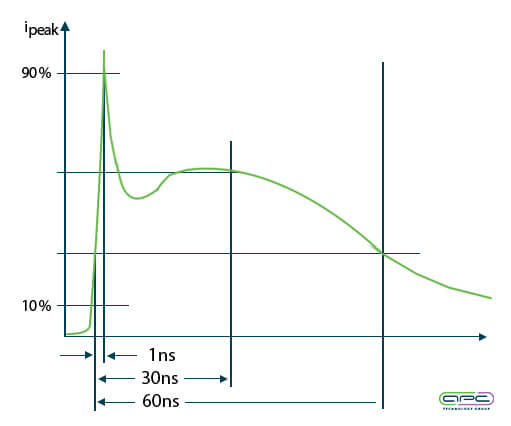

ESD current waveform shape
The IEC/EN 61000-4-2 waveform is a fast, high-current pulse with:
- 0.7–1.0 ns rise time
- Sharp, narrow peak
- Exponential decay over ~60 ns
This shape ensures a consistent and repeatable discharge event across all test generators.
EN 61000-4-2 defines the voltage levels, peak currents, rise times and waveform tolerances required for repeatable system-level ESD immunity testing. These specifications ensure consistent results between accredited laboratories and in-house EMC test facilities.
Discharge tip types used in ESD testing (IEC 61000-4-2)
ESD simulators use interchangeable discharge tips to replicate different real-world static discharge events as defined in EN 61000-4-2. Each tip is designed to control how the ESD pulse couples into the EUT, ensuring repeatable and standard-compliant results.
Common Tip Types:
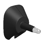

Air Discharge Tip
A rounded, insulated tip used for air-gap breakdown testing. Used for plastic or coated surfaces where contact isn’t possible.
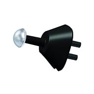

30mm Air Discharge Tip
(for specific applications)
30mm air discharge tip (optional) for specific applications. The 30mm air discharge tip ensures a more stable rise time of the pulse above 15kV.
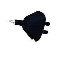

Contact Discharge Tip
A sharp conductive tip that maintains direct contact with the EUT before the pulse is triggered. Provides the most repeatable and preferred method for testing metal surfaces.
ESD test methods (contact, air and indirect)
The EN 61000-4-2 standard defines two main test methods:
- Contact discharge (most repeatable) - Preferred main test method
- Air discharge (for insulating surfaces) - Main test method
ESD test setup
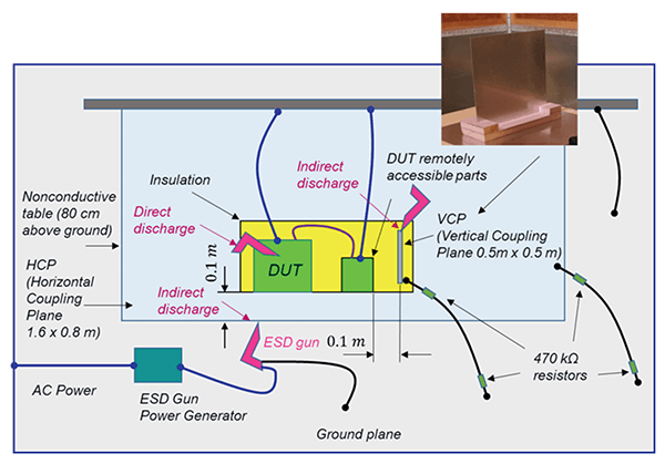
ESD test setups differ depending on the standard and application, but for most commercial products, the configuration is defined by EN 61000-4-2. The standard specifies both a tabletop arrangement for small and medium-sized devices and an alternative configuration for floor-standing equipment that cannot be placed on the ESD test bench.
The diagrams below outline the key elements required by the standard, such as a horizontal coupling plane (HCP) including resistor cables, a vertical coupling plane (VCP) including resistor cables, an ESD test table 160cm x 80cm according to EN 61000-4-2 and an ESD simulator or 'ESD gun'.
Contact discharge method
The contact discharge method involves an ESD simulator making direct, physical contact with a conductive point on the device under test (DUT) to deliver a static discharge. A capacitor in the simulator is charged to a specific voltage and then discharged through a probe that is pressed against the DUT.
This method is preferred for its consistency and speed in testing as it offers the highest repeatability and is the preferred IEC/EN 61000-4-2 test approach for most immunity evaluations.
Overview:
- The tip touches the DUT before the discharge
- Most repeatable
- Preferred method

Air discharge method
The ESD air discharge method involves moving the ESD gun with a rounded tip close to a device at the speed and direction defined in the standard. This method is used when contact discharge is not possible, such as with non-conductive surfaces or when simulating a real-world event where a spark jumps across an air gap. The air gap must be carefully managed for consistency and environmental factors like humidity and temperature can affect the test.
Overview:
- For insulating or curved surfaces
- Arc timing varies with humidity/geometry
- Less repeatable
ESD test equipment
Selecting the right ESD simulator and accessories is one of the most important decisions when setting up an EN 61000-4-2 test environment. Engineers need equipment that matches the standard both electrically and physically, ensuring it’s reliable enough for repeatable testing throughout the entire product development cycle.
At APC Technology Group, we supply a full range of IEC-compliant ESD test generators and coupling-plane accessories and provide expert guidance to help you choose the right equipment for your test setup. Our specialists are available to provide product demos and 1-1 consultations either remotely or in-house, allowing your team to assess usability and discharge performance firsthand before committing to a full in-house setup.


ESD Test Table
160 x 80 cm, made of wood without any metallic parts, as required by EN 61000-4-2.
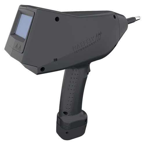

ONYX 16 - ESD Test Gun
Electrostatic discharge test system available in 16 kV or 30 kV versions.


Horizontal Coupling Plane (HCP)
Horizontal coupling plane 1.6 m x 0.8 m for indirect application of the ESD.


Vertical Coupling Plane (VCP)
Vertical coupling plane 0.5 m x 0.5 m, for indirect application of the ESD.


Resistor Cable for ESD
Resistor Cable for ESD, includes 2 x 470 kOhm resistors in cable.
Available in a bundle!
All of the equipment you need for ESD testing in a bundle.
Bring ESD testing in-house with APC
Below are some examples of how APC can support you with your test setup and equipment requirements to fit your long-term testing needs.
|
Voltage range selection - Recommendations are based on both current compliance targets and anticipated future requirements, ensuring long-term suitability |
|
|
Ergonomics and usability – Different generator designs, weights and operational features are evaluated to match your team's workflow and reduce operator fatigue |
|
|
Waveform and calibration – Calibration requirements are explained, along with the verification tools needed to maintain IEC/EN 61000-4-2 waveform accuracy and traceability |
|
|
On-site demonstrations - Demo units can be brought directly to your facility, giving engineers the opportunity to assess ergonomics, discharge behaviour and usability firsthand |
|
|
Support for all IEC setups - Guidance covers both tabletop and floor-standing test configurations defined in IEC/EN 61000-4-2, ensuring compatibility with every product type |
|
|
Full lab planning support - Assistance extends beyond the ESD workstation to help map out wider in-house EMC test capability, including EFT, surge, conducted immunity and emissions |
In-house ESD testing vs external EMC lab testing
Cut outsourcing costs and test on your schedule. APC provides full IEC 61000-4-2 setups, equipment demos, and specialist support.
|
Factor |
In-House Testing |
External Lab Testing |
|
Cost |
One-time equipment cost |
£1,500 - £3,000 per day |
|
Speed |
Immediate testing, no scheduling |
Lab wait time 2-8 weeks |
|
Iteration |
Test immediately after every design change |
Repeated visits required |
|
Debugging |
Real-time, unlimited |
Limited time slots |
|
Accuracy |
Controlled and repeatable |
Accurate but expensive |
|
Best use |
Development, troubleshooting and pre-compliance |
Final certification |
Get expert advice
Request a callback from a member of our technical team to get dedicated one-to-one consultancy for ESD Testing, in-house capability and compliance.
Ready to bring EMC testing in-house?
Whether you're starting from scratch or upgrading an existing test area, APC supplies the full ecosystem of equipment you need to run EMC testing in-house.
From bespoke test chambers to test and measurement equipment and RF systems, APC work with customers directly to reduce outsourcing costs, shorten development cycles and gain full control over pre-compliance testing.
Your partner for reliable and compliant EMC testing solutions
With 40+ years of expertise supporting the electronics industry, APC provides high-reliability components, test equipment and engineering support for organisations building or expanding their EMC and test capabilities. As an authorised distributor for 100+ specialist manufacturers, we supply genuine, traceable equipment backed by recognised certifications.







Resources
ESD Standard Sources:
- Current IEC/EN: IEC/EN 61000-4-2:2025 (3rd Edition)
- Previous: IEC 61000-4-2:2008 (2nd Edition)
Aerospace, Automotive, Medical and Military Standards for ESD Testing:
- Aerospace and Avionics: (DO-160G (Section 25) - ESD testing according to RTCA DO-160D, Section 25
- Military & Defence Electronics: MIL-STD-461- Military Standards: Electromagnetic Interference Characteristics Requirments for Equipment
- Medical Devices & Clinical Electronics: EN 60601-1-2:2015+A1:2021 - Collateral Standard: Electromagnetic disturbances. Requirements and tests
- Automotive ISO: 10605:2023 Road vehicles - Test methods for electrical disturbances from electrostatic discharge
References:
- Figure 1: Comparison of electrostatic discharge models and failure signatures for CMOS integrated circuit devices - Scientific Figure on ResearchGate.
- Figure 2: Comparison of electrostatic discharge models and failure signatures for CMOS integrated circuit devices - Scientific Figure on ResearchGate.
- Figure 3: ESD test setup for table-top equipment - incompliancemag.com
ESD Frequently Asked Questions
What are the typical ESD failure modes?
- Shorted junctions
- Gate oxide rupture
- Metal trace melting
- Electrothermal migration
- Latent semiconductor defects
These failures may appear as resets, no-boots, intermittent faults or total device failure.
Can I perform ESD testing in-house instead of outsourcing?
Yes. Many OEMs and CEMs move ESD testing in-house to:
- Reduce external lab costs
- Shorten development timelines
- Improve first-time pass rates
- Run pre-compliance tests anytime
APC provides full turnkey ESD lab setups, from generators to HCP/VCP tables. Contact a member of our team to learn more.
What is latent ESD damage?
Latent damage occurs when a component is weakened by ESD but does not fail immediately. It may pass production tests and then fail unpredictably in the field. In-house testing catches these early before products reach customers.
What components are most sensitive to ESD damage?
Semiconductors, ICs, MOSFET gates, thin-film resistors, precision capacitors, and SSD/HDD controllers are highly susceptible to both direct damage and latent failures that may only appear after deployment.
What voltage levels are used in IEC 61000-4-2 testing?
The standard defines four contact discharge voltages (2 - 8 kV) and air discharge levels (2 - 15 kV). Higher voltages may be used for robustness or sector-specific standards such as automotive (ISO 10605) or avionics (RTCA DO-160).

